


Page content
A brief description of the instrument
Field emission scanning electron microscopy (FE-SEM) is a more powerful SEM imaging technique widely used in engineering for analysing the surface topography and composition of materials at high magnifications and resolutions. It works by scanning a focused beam of electrons across the sample surface. Wherein electrons detected are processed to form an image, whilst x-rays detected are utilised in elemental analysis. FE-SEM allows engineers to observe nano-scale features in materials or characterise the elemental distribution of materials via EDX.
Uses & Capabilities
This equipment could be used for:
- Semiconductor Inspection (Inspecting microchips to identify defects, contaminants, and structural issues)
- Automotive applications (Inspecting parts, materials, and coatings to identify defects, understanding wear and corrosion thus ensuring durability components)
- Pharmaceutical/Biomedical Industry (Imaging is used for particle morphology characterization, dispersion via EDX and ensuring the quality of drug delivery platforms like microneedle arrays)
- Materials characterisation (Studying the dispersion, distribution, and morphology of fillers/ reinforcements/coatings in composite materials and microstructure, grain boundaries, defects on metals, alloys or ceramics, with additional elemental distribution information gleaned via EDX.
Key capabilities
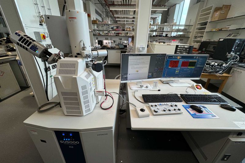
The Hitachi SU5000 is a versatile Schottky field emission scanning electron microscope (FE-SEM) with several useful features and a higher resolution than standard thermionic emission SEM systems. The main additional feature is energy dispersive X-ray spectroscopy (EDX) detector for elemental analysis. Here are some of the key features and specifications:
Key Features
- EM Wizard: An intelligent user interface that provides optimized imaging conditions and automatic adjustments for high resolution and repeatability.
- Variable Pressure Mode: Allows imaging of non-conductive samples without extensive sample preparation by controlling the chamber pressure.
- Large Sample Chamber: Accommodates samples up to 200 mm diameter and 80 mm height.
- Rapid Sample Exchange: Achieves vacuum for observation within 3 minutes or less.
- 3D MultiFinder: Enables easy tilting and rotation of samples while keeping the image centered and in focus.
- Integrated EDX System: Fully integrated EDX detector for elemental analysis and mapping, with seamless switching between SEM and EDX modes.
Specifications
- Resolution: 1.2 nm at 30 kV (high vacuum mode), 3.0 nm at 15 kV (variable pressure mode).
- Accelerating Voltage: 0.5 to 30 kV, with beam deceleration mode for improved low kV performance.
- Detectors: Secondary electron (SE) detector, backscattered electron (BSE) detector, and integrated EDX detector.
- Vacuum Modes: High vacuum and variable pressure modes.
- Magnification Range: Up to 2,000,000X (with optional low magnification mode).
- Additional analytical Capabilities: EDX for elemental analysis and mapping